
Applied Materials stands at the center of the most transformative technology cycle in decades. As the world’s largest semiconductor equipment manufacturer, the company holds approximately 30% of the global wafer fab equipment market — a dominant position that becomes even more valuable as AI-driven chip demand rewrites the rules of semiconductor manufacturing.
Three key investment points make Applied Materials compelling at current levels. First, the company’s unmatched breadth across deposition, etch, and metrology creates switching costs that protect margins and market share. Second, advanced packaging — the critical bottleneck for AI chips — represents a 50%+ growth opportunity in 2026. Third, the structural shift toward gate-all-around transistor architecture positions AMAT’s integrated solutions as essential infrastructure for next-generation chipmaking.
This analysis covers Applied Materials’ business model, industry dynamics, competitive moat, financial performance, valuation, risks, and a clear investment framework for managing this position.
1. Company Overview
Applied Materials designs, manufactures, and sells semiconductor fabrication equipment used to produce virtually every advanced chip on the planet. Founded in 1967 and headquartered in Santa Clara, California, the company has evolved from a single-product startup into a $356 billion market cap leader serving every major chipmaker globally.
Revenue Model and Segment Breakdown
Applied Materials generates revenue through three primary segments:
Segment Q2 FY2026 Revenue YoY Growth Description Semiconductor Systems $5.97 billion +10% Equipment for deposition, etch, CMP, metrology Applied Global Services (AGS) $1.67 billion +17% Spare parts, service contracts, upgrades Display and Adjacent Markets $280 million Varies Display manufacturing, solar equipment
The Semiconductor Systems segment delivers the majority of revenue but AGS provides crucial recurring income with higher margins. The services business benefits from Applied’s massive installed base — when you sell equipment that costs tens of millions per tool, the aftermarket for parts, upgrades, and maintenance becomes substantial.
Customer Base and Market Position
Applied Materials sells to every major semiconductor manufacturer:
– Logic/Foundry: TSMC, Samsung Foundry, Intel Foundry Services, GlobalFoundries
– Memory: Samsung Electronics, SK Hynix, Micron Technology
– Integrated Device Manufacturers: Texas Instruments, Infineon, STMicroelectronics
The customer concentration creates both opportunity and risk. The top five customers typically represent 50-60% of revenue, with TSMC alone often accounting for 15-20%. This concentration reflects industry structure rather than company weakness — there simply aren’t that many companies building cutting-edge fabs.
Geographic Revenue Mix
China represents approximately 24% of Semiconductor Systems and AGS revenue combined, making it a significant but manageable exposure. The company has factored current export restrictions into guidance and expects China revenue to remain “flat to slightly higher” through calendar 2026. Taiwan, South Korea, and the United States comprise most of the remaining revenue.
Institutional ownership stands at approximately 82%, with Vanguard and BlackRock among the largest holders. Insider ownership remains modest at around 0.3%, typical for a mature technology company of this scale.
2. Industry Analysis
2-1. Market Size and Growth Trajectory
The semiconductor equipment industry is entering an unprecedented growth phase driven by artificial intelligence. According to SEMI, global semiconductor equipment sales will reach $156 billion by 2027, up from $130 billion in 2025 — representing a compound annual growth rate of approximately 9%.
More granularly, wafer fab equipment spending on 300mm tools is projected to hit $133 billion in 2026 (+18% year-over-year) and $151 billion in 2027 (+14%). These figures represent upward revisions from earlier forecasts as AI demand consistently exceeds expectations.
The addressable market breaks down by equipment type:
Equipment Category 2026E Market Size Key Players Lithography ~$30B ASML (monopoly in EUV) Deposition ~$25B Applied Materials, Lam Research Etch ~$18B Lam Research, Applied Materials Process Control/Metrology ~$12B KLA, Applied Materials CMP/Planarization ~$3B Applied Materials
Applied Materials competes across all categories except lithography, giving it exposure to roughly $60 billion of the 2026 equipment market. With approximately 30% overall share, the company captures the largest slice of non-lithography spending.
2-2. Structural Growth Drivers
AI Infrastructure Build-Out
The explosion of generative AI and large language models has triggered what Intel CEO Pat Gelsinger calls “the semiconductor industry’s golden age.” Training a frontier AI model requires thousands of GPUs, each containing billions of transistors manufactured with equipment from companies like Applied Materials.
NVIDIA’s data center revenue grew from $15 billion in calendar 2023 to over $100 billion projected for 2026. Every dollar of GPU revenue requires upstream investment in manufacturing capacity. Applied Materials estimates that logic, DRAM, and advanced packaging will account for over 80% of equipment spending growth through 2027.
The ripple effects extend beyond GPUs. AI inference requires memory bandwidth, driving HBM (High Bandwidth Memory) adoption. HBM production involves advanced DRAM processes and sophisticated packaging — both areas where Applied Materials excels.
Gate-All-Around Transistor Transition
The semiconductor industry is transitioning from FinFET to gate-all-around (GAA) transistor architecture starting at the 2nm node. This architectural shift increases equipment intensity per wafer significantly.
GAA transistors require more deposition steps, more etch steps, and tighter process control than FinFETs. Applied Materials’ Integrated Materials Solutions (IMS) approach — combining multiple process steps in a single vacuum chamber — becomes increasingly valuable as transistor complexity rises.
TSMC begins volume GAA production in 2025-2026, with Samsung and Intel following. This transition represents a multi-year tailwind as fabs upgrade equipment for the new architecture.
Advanced Packaging Bottleneck
Perhaps no area presents greater opportunity than advanced packaging. CoWoS (Chip-on-Wafer-on-Substrate) capacity — TSMC’s packaging technology for high-end AI chips — has emerged as the critical bottleneck for GPU supply.
CoWoS capacity has ramped from approximately 15,000 wafers per month in late 2023 to 75,000-80,000 by end of 2025, with targets of 120,000-130,000 by late 2026. Total industry demand for advanced packaging is expected to reach 1 million wafers in 2026.
Applied Materials provides hybrid bonding tools essential for CoWoS and similar packaging technologies. The company’s recent acquisition of NEXX Systems strengthens its panel-level packaging capabilities for even larger AI accelerator packages. Management expects packaging revenue to grow over 50% in calendar 2026.
Geographic Diversification of Semiconductor Manufacturing
Government subsidies from the US CHIPS Act, European Chips Act, and similar programs in Japan, South Korea, and India are driving fab construction globally. Intel’s Arizona and Ohio fabs, TSMC’s Phoenix facility, Samsung’s Texas expansion, and numerous facilities across Europe and Asia all require equipment.
The scale of government investment is unprecedented. The US CHIPS Act alone commits $52 billion to domestic semiconductor manufacturing, with Intel, TSMC, Samsung, and Micron all announcing multi-billion dollar US expansion plans. Europe has committed $43 billion through its Chips Act, while Japan, South Korea, and India each pursue aggressive semiconductor localization strategies.
For Applied Materials, this geographic diversification provides demand visibility even as individual markets experience cyclicality. The company’s Q2 2026 earnings call noted that customers now provide rolling 8-quarter forecasts, enhancing visibility. Additionally, regional diversification reduces dependency on any single geography — even if China restrictions tighten further, robust demand from US, Europe, and allied Asian markets provides an offset.
DRAM and Memory Technology Transitions
While NAND flash memory remains subdued, DRAM is experiencing a renaissance driven by AI workloads. High Bandwidth Memory (HBM) — the specialized DRAM stacked vertically to provide massive bandwidth for GPUs — has emerged as a critical bottleneck alongside advanced packaging.
Applied Materials generated $1.7 billion in DRAM revenue in Q2 2026, up 18% year-over-year. The company leads in wiring, patterning, and peripheral logic steps for memory manufacturing. Management expects these three areas to account for over 80% of equipment spending growth through 2027.
HBM production differs from conventional DRAM in requiring additional through-silicon vias (TSVs) and hybrid bonding steps — both areas where Applied Materials provides essential equipment. As HBM capacity expands to meet GPU demand, Applied captures incremental revenue from these advanced processes.
2-3. Competitive Landscape
The semiconductor equipment industry is an oligopoly. Five companies — ASML, Applied Materials, Lam Research, Tokyo Electron, and KLA — command 56-66% of the total market.
Company Market Cap Primary Strength 2025 Revenue ASML ~$340B EUV lithography (100% share) ~$30B Applied Materials ~$356B Deposition, breadth ~$28B Lam Research ~$120B Etch, NAND ~$16B Tokyo Electron ~$130B Coater/developer, etch ~$18B KLA ~$100B Process control, metrology ~$11B
Applied Materials’ competitive position rests on breadth rather than monopoly. Unlike ASML’s stranglehold on EUV lithography, AMAT competes in multiple categories where alternatives exist. However, its integrated approach creates advantages that pure-play competitors cannot match.
vs. Lam Research: Lam leads in etch equipment, particularly for memory applications. Applied Materials counters with stronger deposition capabilities and broader portfolio coverage. For customers building entire fabs, Applied’s ability to provide more equipment types from a single vendor creates procurement and integration efficiencies.
vs. Tokyo Electron: TEL excels in coater/developer equipment and has strong etch offerings. Applied Materials maintains advantages in PVD, CMP, and metrology. The companies often split equipment orders at major fabs rather than one displacing the other entirely.
vs. KLA: KLA dominates process control and inspection. Applied Materials has invested in metrology but views KLA as more complementary than competitive — both companies sell to the same fabs for different purposes.
3. Economic Moat Analysis
Moat Type 1: Switching Costs and Customer Lock-In
Applied Materials’ deepest moat derives from the enormous switching costs embedded in semiconductor manufacturing. When a fab qualifies a deposition tool for a specific process, that qualification represents months of engineering work and millions of dollars.
Chipmakers cannot casually swap equipment vendors. Each tool requires customized recipes tuned to specific chemistry, temperature, pressure, and timing parameters. These recipes are proprietary and validated through extensive testing. Changing vendors means re-qualifying the entire process — a cost measured in both dollars and production delays.
The evidence appears in customer retention data. Major customers like TSMC, Samsung, and Intel have used Applied Materials equipment for decades. Equipment generations evolve, but vendor relationships persist. A fab that installs Applied’s latest deposition tool almost certainly ran the previous generation as well.
This stickiness explains why equipment market shares remain relatively stable despite intense competition. Once a vendor establishes position in a process step, displacement requires not just better technology but dramatically better technology — enough to justify the switching pain.
Moat Type 2: Technology Leadership and Patent Portfolio
Applied Materials has led PVD (Physical Vapor Deposition) technology development since the 1980s, accumulating over 1,200 PVD-related patents. These patents cover core processes including magnetron sputtering and ion beam deposition, limiting competitors’ ability to enter high-end markets.
The company commands over 80% market share in PVD equipment — a dominance approaching ASML’s lithography monopoly. PVD tools deposit thin metal films essential for chip interconnects. As transistors shrink and interconnect layers multiply, PVD importance grows.
In CVD (Chemical Vapor Deposition), Applied holds approximately 30% market share in a $13 billion market, competing with Lam Research (21%) and Tokyo Electron (19%). While not monopolistic, this position in the largest deposition category provides substantial revenue.
Moat Type 3: Integrated Materials Solutions (IMS)
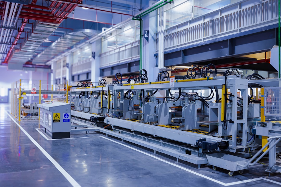
Applied Materials’ unique capability involves combining multiple process steps within a single vacuum chamber. This Integrated Materials Solutions approach reduces air breaks between processes, improving yields and throughput while reducing contamination risk.
For advanced nodes like GAA, where dozens of process steps build three-dimensional transistor structures, integration becomes critical. A customer using Applied’s IMS platform can perform deposition, treatment, and metrology without exposing wafers to atmosphere between steps.
Competitors typically specialize in individual process steps. While they may excel at etch or deposition in isolation, they cannot offer the integrated workflow that Applied provides. This integration moat strengthens as chip complexity increases.
Moat Durability Assessment
Applied Materials’ moats should persist for at least the next 5-10 years, though they face specific threats:
Risk to switching cost moat: A paradigm shift in semiconductor architecture could reset vendor positions. However, GAA transistors and advanced packaging both favor Applied’s existing strengths rather than disrupting them.
Risk to technology moat: Continued R&D investment is non-negotiable. Applied spends approximately $3 billion annually on R&D, maintaining technology leadership. A significant miss in a key technology transition could erode position.
Risk to integration moat: Competitors could develop their own integrated platforms. Lam Research has moved in this direction. However, Applied’s 50+ year head start and broader portfolio create barriers to replication.
On balance, the moats appear durable. The structural trend toward increased equipment intensity per wafer — more steps, tighter tolerances, more complex 3D structures — plays to Applied Materials’ strengths.
4. Financial Analysis
Revenue and Profitability Trends
Applied Materials has delivered steady growth through semiconductor cycles:
Fiscal Year Revenue Operating Income Net Income Gross Margin FY 2022 $25.79B $7.79B $6.53B 46.5% FY 2023 $26.52B $7.65B $6.86B 46.7% FY 2024 $27.18B $7.87B $7.18B 47.5% FY 2025 $28.37B $8.29B $7.00B 48.7% TTM (Apr 2026) $29.02B $8.30B $8.51B 49.0%
Revenue grew from $25.8 billion in FY2022 to $29.0 billion TTM, a 12% cumulative increase despite China export restrictions taking effect mid-period. More importantly, gross margins expanded from 46.5% to 49.0% — a 250 basis point improvement reflecting pricing power and mix shift toward higher-margin advanced equipment.
Q2 FY2026 Performance (Record Quarter)
The most recent quarter demonstrated the business at peak performance:
– Revenue: $7.91 billion (record, +13% sequentially, +11% YoY)
– Semiconductor Systems: $5.97 billion (record)
– Applied Global Services: $1.67 billion (+17% YoY)
– Non-GAAP Gross Margin: 50% (+80 bps YoY)
– Non-GAAP EPS: $2.86 (beat $2.66 consensus by 7.5%)
The beat extended Applied’s streak to four consecutive quarters exceeding analyst expectations. More significantly, the margin expansion indicates pricing strength — customers are paying premium prices for Applied’s equipment amid tight supply.
Balance Sheet and Cash Flow
Applied Materials maintains a fortress balance sheet:
– Cash and Equivalents: ~$8 billion
– Total Debt: ~$6 billion
– Net Cash Position: ~$2 billion
– Free Cash Flow (TTM): ~$7 billion
The company generates substantial free cash flow, enabling aggressive capital returns. Applied has repurchased over $20 billion of stock over the past five years while maintaining a dividend that yields approximately 0.7% at current prices.
Q3 FY2026 Guidance (Acceleration)
Management guided Q3 to:
– Revenue: $8.95 billion (+/- $500M) — implies 13% sequential growth at midpoint
– Non-GAAP EPS: $3.36 (+/- $0.20) — implies 17% sequential growth at midpoint
If achieved, Q3 would set another revenue record and demonstrate accelerating momentum. Management noted that equipment spending is expected to grow “more than 30%” in calendar 2026, with advanced packaging growing “over 50%.”
5. Valuation
Current Metrics
At $448.25 per share, Applied Materials trades at:
Metric Value Market Cap $355.7 billion P/E (TTM) 42.2x P/E (Forward, CY2026E) ~28x EV/EBITDA (TTM) ~27x Price/Sales (TTM) 12.3x Price/FCF ~51x
The trailing P/E of 42x appears elevated, but forward estimates paint a different picture. Analysts project approximately $16 EPS for calendar 2026, implying a forward P/E of 28x — reasonable for a company growing earnings 20%+ annually.
DCF Valuation Framework
Using conservative assumptions:
– Revenue Growth: 15% CAGR over 5 years (below management’s 30%+ 2026 guidance)
– Operating Margin: 30% terminal (currently ~29%)
– Tax Rate: 12% (current effective rate)
– WACC: 10%
– Terminal Growth: 3%
This yields an intrinsic value range of $480-$550 per share, suggesting 7-23% upside from current levels.
Price Target Scenarios
Scenario 2026E EPS Multiple Price Target Upside Bear Case $14.50 25x $363 -19% Base Case $16.00 30x $480 +7% Bull Case $17.50 35x $613 +37%
Bear case assumes semiconductor capex moderates faster than expected, China restrictions tighten further, and multiple compression from current levels.
Base case assumes management guidance accuracy, continued margin expansion, and stable valuation multiples consistent with growth rates.
Bull case assumes advanced packaging and GAA transitions drive upside to estimates, with multiple expansion as AI spending durability becomes clearer.
Analyst Consensus Comparison
Wall Street consensus price target stands at $510.77, representing 14% upside. Recent upgrades following Q2 earnings:
Firm Target Rating Cantor Fitzgerald $575 Overweight Deutsche Bank $550 Buy BofA $540 Buy Citi $520 Buy Morgan Stanley $502 Overweight
The base case target of $480 sits below consensus, reflecting a more conservative stance on near-term multiple expansion. However, the fundamental thesis aligns with the Street’s bullish view.
6. Risk Factors
Risk 1: China Export Restrictions
China represents 24% of Applied Materials’ semiconductor-related revenue, making export policy a material risk. The US has implemented increasingly strict controls on semiconductor equipment sales to Chinese customers, particularly for advanced manufacturing.
Applied has incorporated current restrictions into guidance, but policy could tighten further. Complete exclusion from China would remove roughly $7 billion of annual revenue — a scenario that would significantly impact earnings even if partially offset by demand elsewhere.
Mitigation factors include geographic diversification of demand, US CHIPS Act subsidies supporting domestic capacity, and Applied’s exposure being weighted toward mature-node equipment less affected by restrictions. However, the risk remains substantial and largely outside management’s control.
Risk 2: Semiconductor Cycle Volatility
Semiconductor equipment spending is notoriously cyclical. The industry experienced a downturn in 2019 and again in 2022-2023 following pandemic-era overbuilding. While current AI-driven demand appears structural, history cautions against assuming immunity from cycles.
A recession that reduced enterprise IT spending could slow data center buildouts, potentially triggering equipment order cancellations or delays. Memory pricing weakness — currently masked by HBM strength — could resurface if AI demand disappoints.
Applied’s diversification across logic, memory, and packaging provides some buffer, as does the services business providing recurring revenue. However, a severe downturn would impact results regardless of business mix.
Risk 3: Customer Concentration and Capex Dependency
Applied Materials’ largest customers are themselves making enormous capital allocation decisions. TSMC’s 2026 capex budget exceeds $30 billion; Intel’s restructuring involves tens of billions in fab investments; Samsung’s memory and foundry roadmaps require massive spending.
If any major customer significantly reduces capital spending — whether from financial stress, demand weakness, or strategic pivot — Applied would feel the impact immediately. The company cannot easily replace a customer spending $4-5 billion annually on equipment.
This risk is inherent to the equipment business model. Applied mitigates it through long-term customer relationships, multi-year visibility from rolling forecasts, and the essential nature of its products — customers may delay spending but cannot abandon it entirely while remaining competitive.
Risk 4: Technology Disruption and Competition
While Applied Materials holds technology leadership today, semiconductor manufacturing evolves rapidly. The transition from FinFET to GAA transistors represents both opportunity and risk — Applied must execute flawlessly to capture the incremental equipment intensity while fending off competitors also targeting this transition.
Lam Research, in particular, has invested heavily in expanding beyond its etch stronghold. Tokyo Electron continues to gain share in select deposition categories. A technology misstep by Applied — being late to market with a critical GAA tool, for example — could allow competitors to establish beachheads.
Applied’s $3 billion annual R&D budget provides some insurance, but semiconductor equipment requires not just R&D spending but the right R&D bets. The company’s track record suggests strong technology roadmap execution, but past performance does not guarantee future success in an industry where technology leadership can shift within a single product generation.
7. Conclusion and Investment Framework
Investment Rating: Buy
Applied Materials represents a core holding for investors seeking semiconductor exposure. The company’s dominant market position, technology leadership, and exposure to structural growth themes — AI infrastructure, advanced packaging, GAA transitions — create a compelling long-term profile.
Entry Considerations
The current price of $448.25 sits approximately 3% below the 52-week high of $462.40, suggesting limited near-term margin of safety. However, accelerating fundamentals (Q3 guidance implies continued momentum) support the valuation.
– Ideal entry range: $400-$430 (10-20% below current levels on market weakness)
– Acceptable entry: Current levels for long-term positions
– Avoid entry: Above $480 without additional positive catalysts
Exit Framework
Target achieved — trim position:
– Take 25% profit at $520 (base case target, ~16% upside)
– Take additional 25% at $575 (bull case scenario)
– Maintain 50% core position for long-term compounding
Fundamental break — reassess position:
– Gross margins decline below 46% for two consecutive quarters
– China revenue drops below 15% without offsetting demand elsewhere
– Major customer (TSMC/Samsung/Intel) announces significant capex cuts
– Management lowers full-year guidance below 20% equipment growth
Time-based review:
– Reassess thesis in 6 months (November 2026)
– Key events to monitor: Q3 earnings (August), SEMICON West conference, major customer capex announcements
Summary Table
Item Detail Company Applied Materials (AMAT) Current Price $448.25 Base Case Target $480 Bull Case Target $613 Bear Case Target $363 Upside (Base) +7% Rating Buy Key Thesis AI-driven equipment supercycle, 30%+ market share, advanced packaging bottleneck beneficiary Main Risk China export restrictions, semiconductor cycle volatility
—
Disclaimer
This article is for informational purposes only and does not constitute investment advice. All data sourced from public filings, analyst reports, and news as of the publication date. The author may hold positions in securities mentioned. Invest at your own discretion and conduct your own due diligence before making investment decisions.
함께 읽으면 좋은 글
- American Express Closed-Loop Network Advantage: Why Premium Card Spending Growth and 34% ROE Make AXP a Warren Buffett Favorite
- Alphabet’s Google Cloud AI Growth Investment Thesis 2026: Why the $460 Billion Backlog Makes This a Core Holding
- Seagate HAMR Mozaic 4+ 44TB Hyperscaler Adoption: Why the AI Storage Supercycle Makes This a $1,000 Stock
- Amazon AWS AI Infrastructure Investment Thesis 2026: How the $150 Billion Cloud Giant Is Building the Backbone of the Agentic Economy
- [2026 May Reanalysis] AMD Base Target Reached: Q1 Data Center Revenue Surges 57% to $5.8 Billion as Stock Hits All-Time High — Executing Partial Profit-Taking at $467